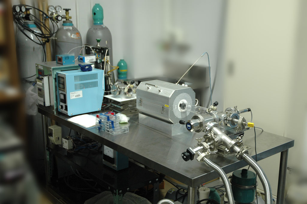
Ethanol CVD (home made)
(Ethanol Chemical Vapor Deposition)
Used for carbon nanotube growth (mostly single-walled nanotubes).
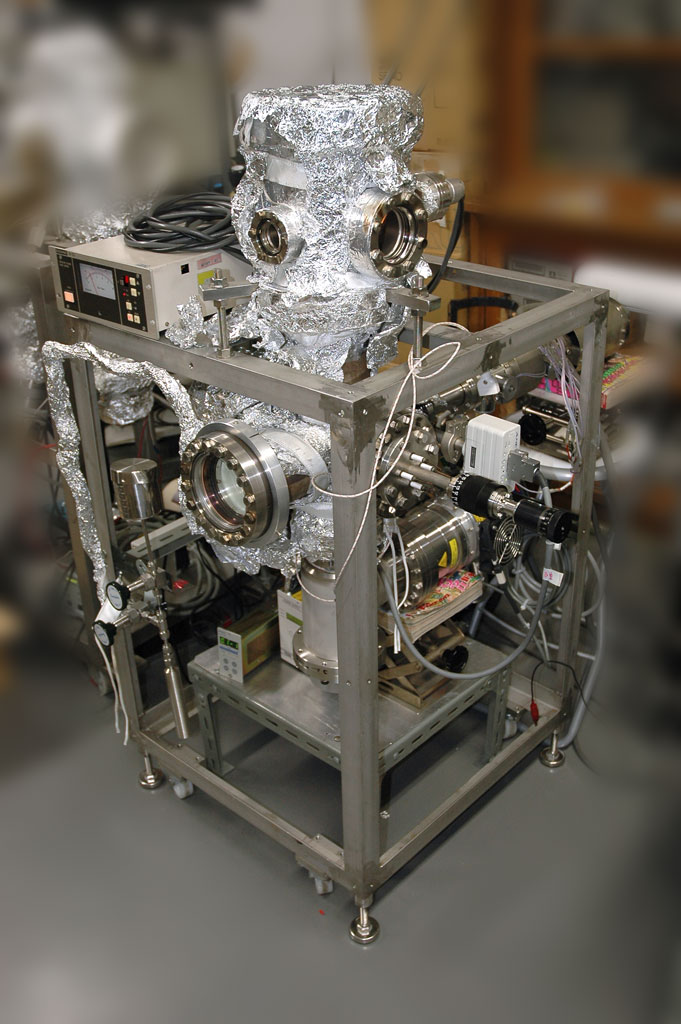
CVD/RHEED (home made)
(Chemical Vapor Deposition/Reflection High-Energy Electron Diffraction)
Used for determination of crystal structures of growing nanotubes and their catalyst.
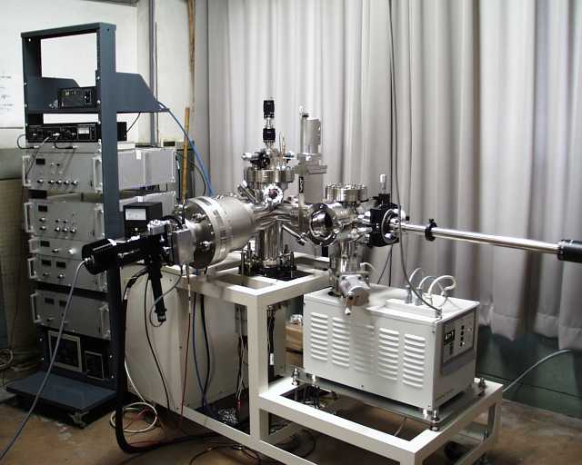
RHEED/AES (Staib)
(Reflection High-Energy Electron Diffraction/Auger Electron Spectroscopy)
Used for graphene growth under inert gas environment.
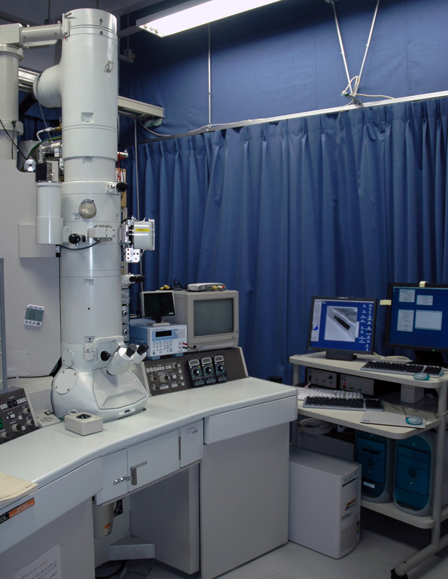
TEM (JEOL)
(Transmission Electron Microscope)
Used for observation of CNT/graphene in an atomic resolution, it is also possible to observe in-situ field emission of CNTs.
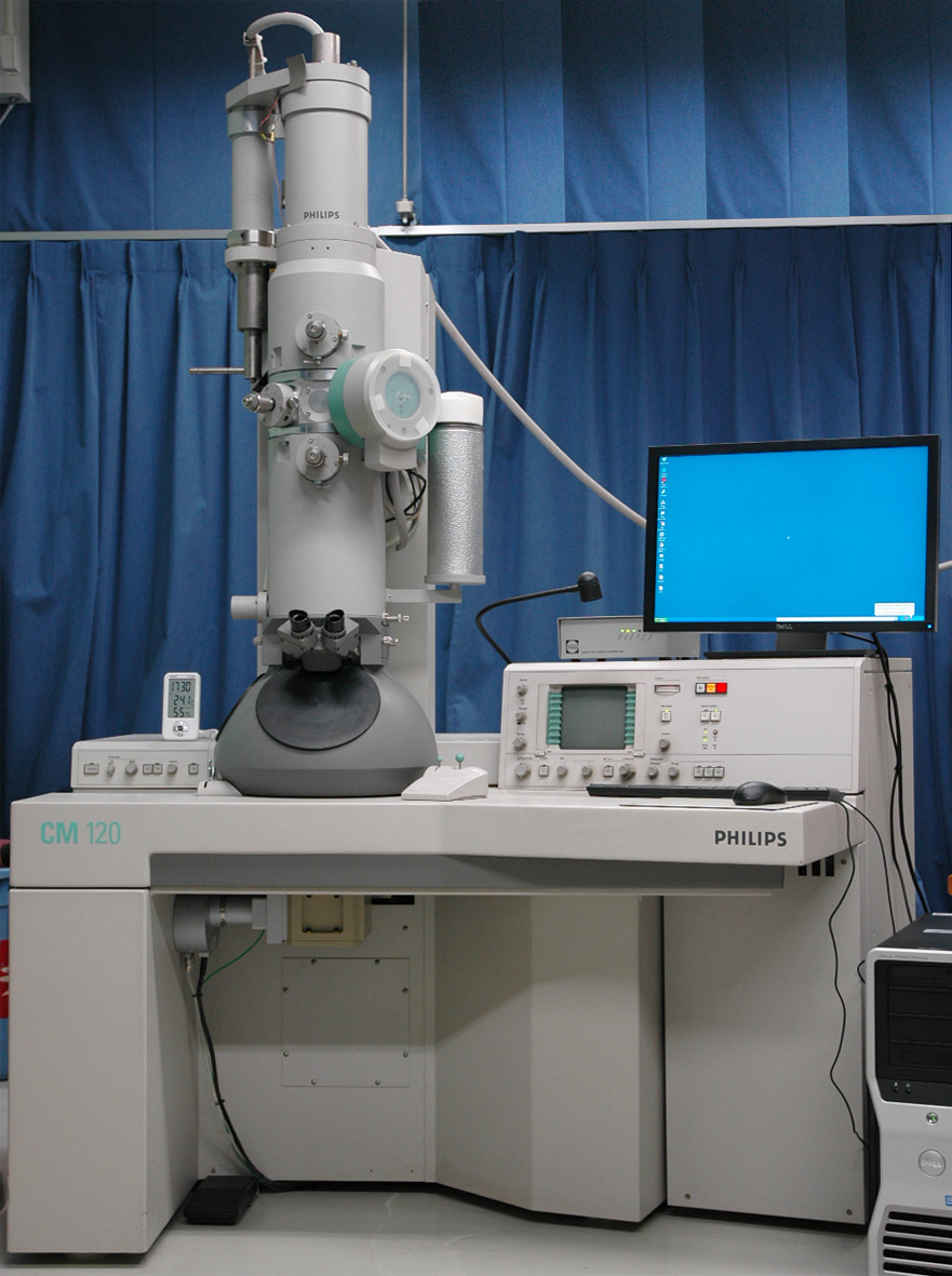
TEM (FEI)
(Transmission Electron Microscope)
Used for high resolution observation of CNT/graphene.
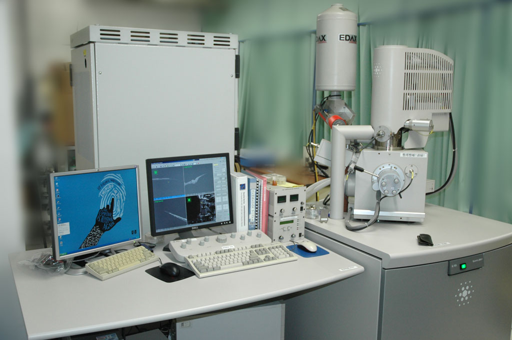
E-SEM (FEI)
(Environmental Scanning Electron Microscope)
Mainly used for CNT/graphene manipulation under SEM observation.
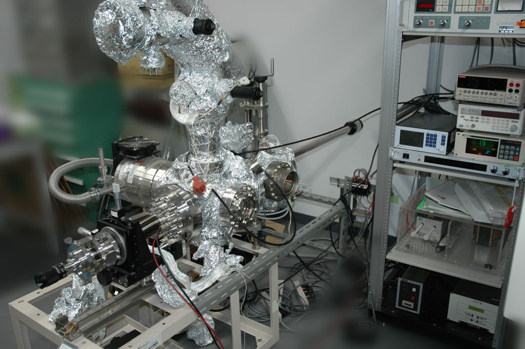
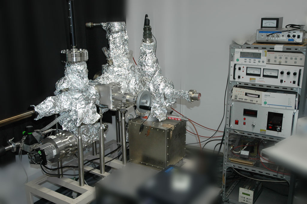
FEM (home made)
(Field Emission Microscope)
Used for observation of CNT tip structure, it can investigate effects of gas molecules and metal deposits to the CNT field emissions.
FEM/FIM (home made)
(Field Emission Microscope/Field Ion Microscope)
This apparatus has a function to observe a CNT tip in atomic resolution in addition to FEM function.
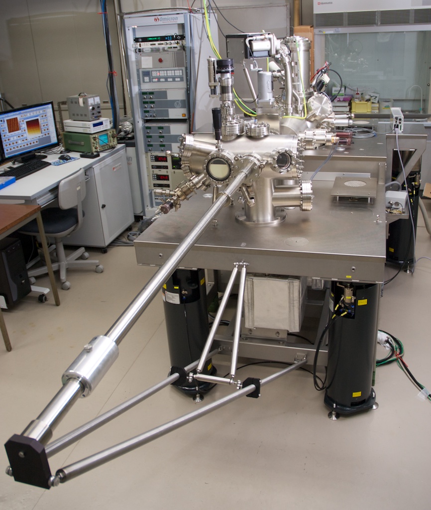
4-Probe STM/SEM (Omicron)
(4-Probe Scanning Tunneling Microscope/Scanning Electron Microscope)
Mainly used for structural and morphological observation of graphene films, it can also investigate electrical properties of the films.
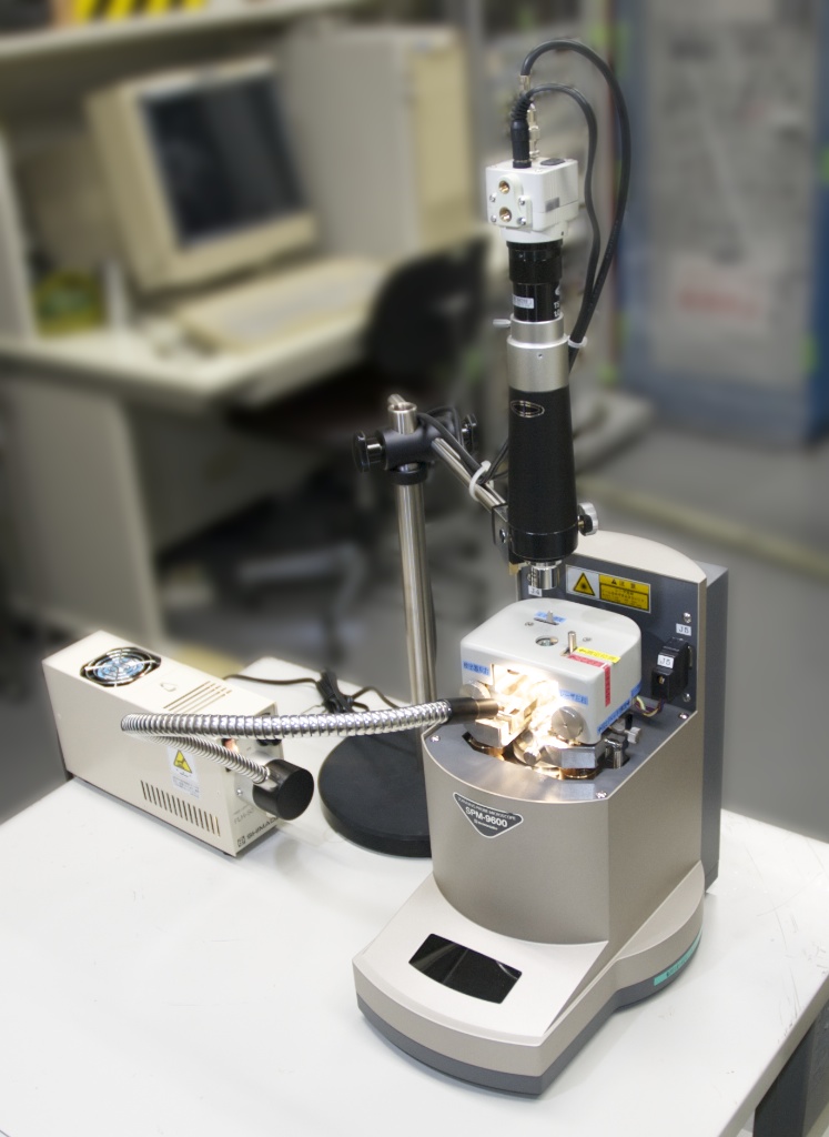
AFM (Shimadzu)
(Atomic Force Microscope)
Mainly used for morphological observation of graphene films.
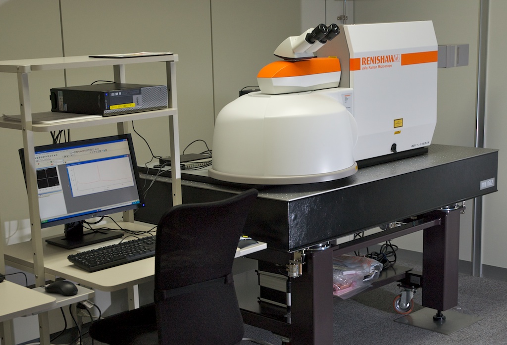
μ-RAMAN (Renishaw)
(Microscopic Raman Spectroscopy)
Used for determination of diameter of CNT and layer number of graphene.