Outline of the ResearchWe are studying on nano-scaled materials (such as carbon nanotubes etc.) and surface and interface (low-dimensional) structure of semi-conductors and metals. Transmission electron microscopy (TEM), scanning tunneling microscopy (STM), reflection high-energy electron diffraction (RHEED), X-ray diffraction (XRD), synchrotron radiation (SR) are our main tools. In addition to reveal a new physics on such materials, applications of nano materials to electronic devices are also studied.Research Themes
Links to the each theme
Publication List |
 Model Picture of a Double Wall Carbon Nanotube (DWNT) 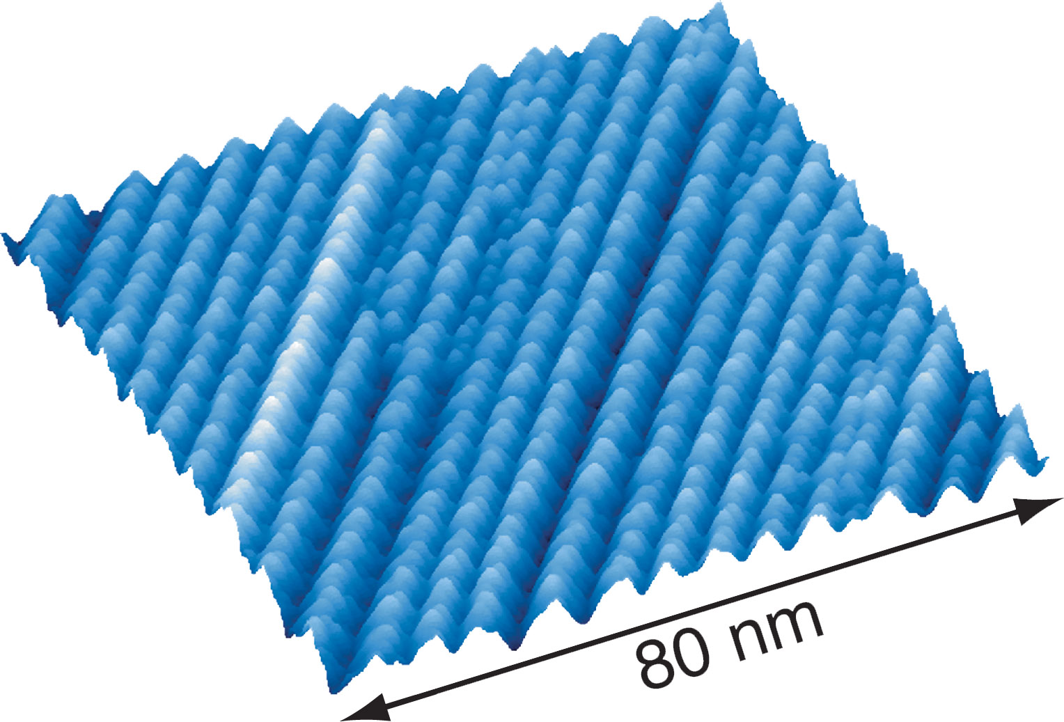 STM Image of a Self-Organized Surface Nano Structure (Ga on Si(113) Surface) |